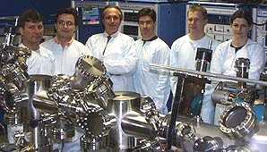
Photogenic Group
Development of quantum-scale semiconductor heterostructures and exploratory materials
for novel high efficiency photovoltaic devices
 Photogenic Group |
Development of quantum-scale semiconductor heterostructures and exploratory materials
for novel high efficiency photovoltaic devices |
Current tasks within the group include:
Chemical Beam Epitaxy of Quantum-Scale Heterostructures and Devices for Advanced Photovoltaics:
High Efficiency Multi-Bandgap/Multiquantum Well Photovoltaics for Satellites Operating in Low and Geostationary Earth Orbit:
Radiation Hard InP Multiquantum Well Solar Cells for Medium Earth Orbit Applications:
Thermophotovoltaic Materials and Converters for Deep Space Exploration:
Solar Cells Using Extraterrestrial Planetary Resources:
Major Research activities include the design and modeling of photovoltaic devices,
growing crystalline semiconductors by chemical beam epitaxy (CBE/MOMBE),
characterizing critical material properties that affect cell efficiency and reliability,
developing cell processing and fabrication techniques, and measuring the photovoltaic response of
completed solar cells. Project capabilities include growing quantum-scale heterostructures and
devices by CBE/MOMBE; complete device processing facilities; and structural and electrical
characterization tools such as X-ray diffraction, electron microscopy C-V profiling, and
photoluminescence. Device photovoltaic characterization facilities include dark-illuminated I-V
(AM0 solar simulator) and spectral response analysis.
Patents
Tandem Solar Cell With Improved
Tunnel Junction
Alexandre Freundlich
Mauro F. Vilela
Abdelhak Bensaoula
Alex Ignatiev
Tandem Solar Cell With Indium Phosphide
Tunnel Junction
Mauro F. Vilela
Abdelhak Bensaoula
Alexandre Freundlich
Philippe Renaud
Nasr-Eddine Medelci
Strained Quantum Well Photovoltaic
Energy Converter
Alexandre Freundlich
Philippe Renaud
Mauro F. Vilela
Abdelhak Bensaoula
Multi-Quantum Well Tandem Solar
Cell Patent Front Page
Alexandre Freundlich
Quantum Well ThermoPhotovoltaic
Energy Converter
Alexandre Freundlich
For more information contact
Project Leader:
Professor Alex Freundlich at
alexf@orbit.svec.uh.edu
Last modified: 28 July 2001