The present invention relates to quantum well semiconductor light emitting
devices such as lasers that utilize resonant tunneling for carrier injection
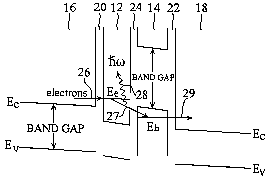
and spatially-diagonal transitions between an energy state in the conduction
band of one quantum well and an energy state in the valence band of the
adjacent quantum well for light emission, resulting in much improvement in
both radiative efficiency and carrier injection efficiency. An elementary
structure of the invented devices comprises two spatially coupled quantum
wells residing in conduction and valence bands respectively wherein the
valence band-edge in one quantum well is higher than the conduction band-edge
of the other quantum well. Each quantum well contains at least one energy
state formed by the quantum size effect. Light emission occurs by the
transition of electrons from the state which is higher in energy in the
conduction band quantum well to the state in the valence band quantum well,
and the emission wavelength is inversely proportional to the energy difference
between the two states which can be easily tailored by adjusting quantum well
thicknesses. Cascade emission is realized in a superlattice structure which
is constructed by periodically stacking many repeated elementary device
structures.